In February 2026, India joined the Pax Silica Declaration, a US-led supply-chain framework designed to secure mainly critical minerals and semiconductors (also known as chips). Prior to that, the Indian government established India Semiconductor Mission (ISM) in 2021 to strengthen the domestic semiconductor ecosystem by about 10 billion US dollars of subsidy. For years, India’s semiconductor ambition has attracted less attention than the equivalents in the USA, EU, Japan and South Korea. As American memory giant Micron Technology started its manufacturing in Gujarat in February 2026, India’s ambitions seem to finally start making progress with international and domestic supports. In this article, I will try to explain where India is standing in the semiconductor industry now and how it will impact the national securities in the Indo-Pacific region.
India’s Current Position in the Semiconductor Industry
The semiconductor industry is like a huge jungle which has millions of species. To make it more comprehensible, I’ll try to summarize the current main players (Taiwan, South Korea, the USA, Japan, Europe, China and India) indispensability in six categories (Advanced Logic Front End, Memory Front End, Back End, Photolithography Equipment, Other Equipment, Material). “Front-End” is making the circuits on the silicon wafer. In this article, I confined Front End to advanced logic (sub 7nm) and memory chips since these two kinds of chips are most crucial to AI/Data server. “Back End” is to cut the chip from the wafer and make a package. “Photolithography” is the most crucial front-end process used to manufacture advanced microchips. “Other Equipment” is used to make films, etch the films, polish the wafer, etc. And each step use hundreds of materials from organic polymers to industrial gases.
Although there is a design section in the industry and India has some presence in the section, it is hard to quantify because of diversified business models (designing the circuit, design software development, IP sales, etc), I focused on actual manufacturing sections.
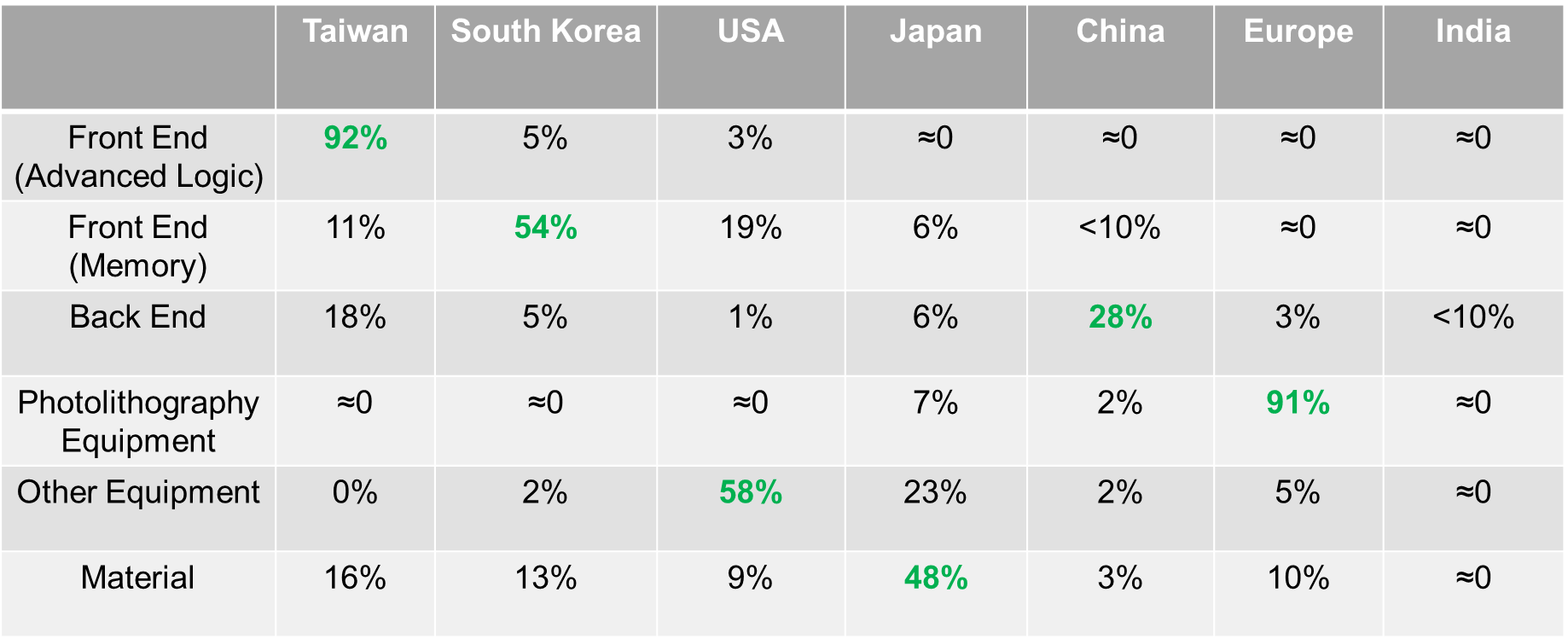
India’s current presence in the semiconductor industry is smaller than any other selected region in 2026. Although 20% of global design talent were from India in 2025, actual manufacturing (front end and back end), chipmaking equipment and chemical material industry require different kinds of skillsets; meticulous each process parameter’s optimization, integration of hundreds of steps, sustaining stable material supply and equipment maintenance. Without momentum from outside, it’s not as simple as just transferring people from one section to another.
India’s Ambitious Strategy
Although ISM’s initial budget was about 10 billion US dollars, total investment became about 18 billion US dollars and ten projects had been approved by September 2025. In addition to the Micron’s packaging and test center (back end) in Gujarat, the Indian conglomerate Tata group (Tata Electronics) and Taiwanese foundry Powerchip Semiconductor Manufacturing Corporation (PSMC) will make a front end fab in Gujarat which aims to make 28 nm ~ 120 nm logic and analog chips ― which tend to be used for appliances, automobiles and industrial machines. Tata Electronics is planning to make a back end factory in Assam as well. When both Tata’s factories become operable, India will be able to integrate the front end and back end inside the country.
The Outlook
Manufacturing: Realistic but Smart Focus on the Back End
Looking through the list of approved and pending approval projects, one thing is obvious: more than half of the projects are back-end projects. This strategy is realistic and likely to work in a short timeline in a country like India ― a country which has a huge population and weaker infrastructure than that of other chip-making countries in East Asia countries and the USA.
Chip making process can be divided into three phases design, front end and back end. The design section is designing the function and design of the chips using software called Electronic Design Automation (EDA). This section doesn’t have to handle tens of thousands of actual wafers every month. Although both the front end and back end are critical to mass production and supply chain strategy, they differ significantly in their infrastructural demands. More precisely, front end has more rigorous criteria.
Chip making processes unfold in an incredibly tiny, even nano-meter world, (nano-meter is one billionth of a meter (1 × 10⁻⁹ m)). In International Organization for Standardization (ISO) classification, semiconductor manufacturing front end is categorized in Class 1~3, which is stricter than pharmaceutical manufacturing. ISO Class 1 allows only 10 particles ( ≥ 0.1 μ m ) per cubic meter which is comparable to a situation in which a single dust particle about 1/1000 of the diameter of a human hair exists in a cubic foot of space. On the other hand, back end is categorized in Class 6~8, since chip surfaces are already protected by resin. To keep the extremely clean environment, front end factories need high functional air filter air flow controllers and pressure controllers ― the clean room’s pressure is kept higher than outside so that no air can go in ― working 24/7. Single momentary power outage causes catastrophic problems to chips factories, especially front-end factories.
India’s System Average Interruption Frequency Index (SAIFI) ―the standard metric used by electric utilities to measure how often the average customer experiences a power outage over a specific period, usually a year ― was
137.86 outages/year in 2024, while Taiwan’s SAIFI was 0.209 in 2024. Although India’s SAIFI has kept going down, 136.86 is too high to remain operational, as sensitive wafer surfaces are far more vulnerable to disruption than in back-end processing. Focusing on back end factories rather than front end fab is a realistic target to achieve in a short time period (up to five years) based on India’s current infrastructure level.
Equipment and Materials: Trap of the “Copy Exact”
On the other hand, the outlook for the chipmaking equipment and materials is not as promising as back end factories because of the industry’s key word problem. “Copy Exact” is a key word every engineer in this industry has heard. In nano meter world, any tiny difference could make a huge yield loss, even if the specification of the equipment or material is exactly equal. For example, companies A and B offer chemical C and both specifications show its purities are 99.9% because it’s the limit of the purity measurement equipment. But in reality, company A’s actual chemical purity could be 99.99% while company B’s could be 99.91%. And only company A’s product can contribute to the product yield per wafer in the semiconductor factory. This is a frequent situation in the semiconductor industry. So, among the engineers, using materials or equipment which have already proved to be successful in the past is the safest way when launching a new product or factory. And Both the equipment and materials industries are already controlled by an oligopoly of a few American, Japanese, and European companies. For India ― a country which is seeking entry into the semiconductor industry ― there’s huge hurdles to establish equipment and material industry domestically and it is easier and safer to buy proven products from American, Japanese and European companies. Once India’s chips industry successfully starts making chips with these companies’ equipment and materials, “copy exact” mindset sets in again when India tries to make a newer generation of chips. The prevailing mentality is, “We are making chips using these equipment and materials, why change them, risk a gamble.”
Unlike China, India has a good relationship with these countries and most of the major companies from these countries are launching new offices in India. Although this wouldn’t be an imminent problem, it is likely to be difficult for India to launch in equipment and material field.
From Geopolitical Perspective
Integrating India into Western semiconductor supply chain would strengthen the resilience of Western industry with minimum risks. Here’s why: 1) Considering the difficulty of sub 7 nm front end processes and India’s still-weak infrastructure, Taiwan, South Korea and the US can focus on the top-notch chips for AI and data server while securing via India’s inclusion an additional legacy chips supply for appliances, automobile and industrial robots. 2) India will likely remain depending on Western equipment and materials which can be used as political levers. 3) As a direct consequence of this reliance, it’s unlikely that Indian chips or technical knowledge would flow into unclear country like Russia.
Considering current chips-related geopolitical tensions and Western countries’ willingness to help, India will likely exhibit a huge presence in back end factories and make some progress in front end while maintaining its existing status as design engineer supplier and equipment/material buyer. This rise will likely strengthen the resilience of the Western chips supply chain and become a new variable in ongoing US-China tech war. While China has struggled in top-notch front end fabrication, it has a huge presence in back end phase of legacy chips with its global share of 28% in 2026. Diversifying the back end supplier will mitigate economic leverage threats—similar to how Russia and Iran use energy—regardless of which chip generation India focuses on.





.svg.avif)